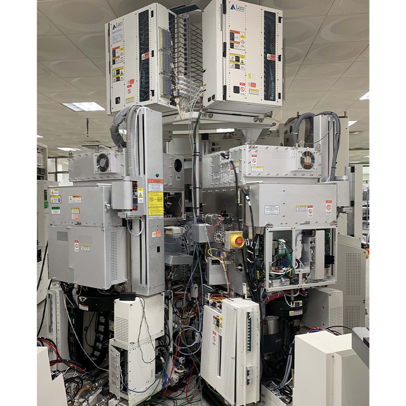
半导体材料是一类导电性能介于导体与绝缘体之间的材料,其电阻率约在1mΩ·cm~1GΩ·cm范围内。这类材料在电子工业、信息技术和新能源技术等领域具有广泛的应用。以下是关于半导体材料的详细介绍:
半导体材料可以根据其化学组成和晶体结构进行分类,主要包括以下几类:
半导体材料在各个领域都有广泛的应用,主要包括以下几个方面:
随着科技的不断发展,半导体材料也在不断更新换代。未来半导体材料的发展趋势主要包括以下几个方面:
Semiconductor materials are a type of material with conductivity between conductors and insulators, with a resistivity ranging from approximately 1m Ω· cm to 1G Ω· cm. This type of material has a wide range of applications in fields such as electronics industry, information technology, and new energy technology. The following is a detailed introduction to semiconductor materials:
1、 Definition and Characteristics
Definition: Semiconductor materials refer to materials with conductivity between conductors and insulators at room temperature. They possess unique electrical, optical, and thermal properties and are the cornerstone of modern electronic technology.
Characteristics: The conductivity of semiconductor materials can be controlled by doping impurities, changing temperature, lighting, and other conditions. In addition, they also possess unique physical properties such as photoelectric effect, rectification effect, thermoelectric effect, etc.
2、 Classification
Semiconductor materials can be classified based on their chemical composition and crystal structure, mainly including the following categories:
Elemental semiconductor: A semiconductor material composed of a single element, such as silicon (Si), germanium (Ge), etc. Silicon is the most commonly used elemental semiconductor material, widely used in fields such as integrated circuits and solar cells.
Compound semiconductor: A semiconductor material composed of two or more elements, such as gallium arsenide (GaAs), indium phosphide (InP), etc. This type of material has important applications in high-frequency, high-speed electronic devices and optoelectronic devices.
Organic semiconductor: Semiconductor materials composed of organic molecules, such as naphthalene, anthracene, etc. This type of material has the advantages of low cost, good solubility, and easy processing, but it is still in the research stage.
Amorphous semiconductor: also known as amorphous semiconductor or glass semiconductor, its atomic arrangement does not have a long program. This type of material has potential applications in fields such as solar cells and liquid crystal displays.
3、 Application
Semiconductor materials have a wide range of applications in various fields, mainly including the following aspects:
Integrated circuit: Semiconductor materials are the basic materials of integrated circuits, and various integrated circuit chips with specific functions can be produced through doping and microfabrication techniques.
Optoelectronic devices: Semiconductor materials have important applications in optoelectronic devices, such as light-emitting diodes (LEDs), laser diodes, etc. These devices utilize the photoelectric effect of semiconductors to emit and receive optical signals.
Solar cells: Semiconductor materials are one of the key materials in solar cells, which convert solar energy into electrical energy through the photoelectric effect.
Sensors: Semiconductor materials can also be used to make various sensors, such as temperature sensors, pressure sensors, light sensors, etc. These sensors have a wide range of applications in industrial automation, medical instruments, and other fields.
4、 Development Trends
With the continuous development of technology, semiconductor materials are also constantly being updated and replaced. The future development trends of semiconductor materials mainly include the following aspects:
The research and development of new semiconductor materials, such as two-dimensional materials (graphene, transition metal chalcogenides, etc.) and quantum dot materials, have unique physical properties and broad application prospects.
Integration of semiconductor materials: With the continuous development of integrated circuit technology, the integration degree of semiconductor materials will continue to improve to achieve higher performance and lower power consumption.
The greenization of semiconductor materials: Environmental protection and sustainable development are important directions for future technological development, so the research and application of green semiconductor materials will also become an important trend.
全国服务热线
18030183032
邮 箱:3248602330@qq.com
地 址:厦门市思明区吕岭路1733号创想中心2009-2010单元
Copyright © 2022-2024 厦门雄霸电子商务有限公司 版权所有 备案号:闽ICP备14012685号-38


18030183032